Microsoft reveals HoloLens Holographic Processing Unit has 24 cores capable of 1 trillion FLOPS
2 min. read
Published on
Read our disclosure page to find out how can you help MSPoweruser sustain the editorial team Read more
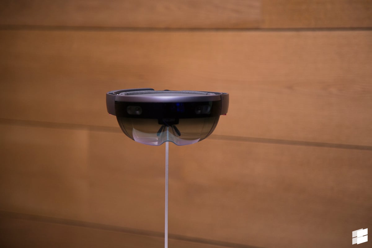
Microsoft HoloLens is the world’s first fully self-contained, holographic computer, enabling users to interact with high-definition virtual holograms in the real world. The secret sauce of Microsoft HoloLens is its Holographic Processing Unit, a custom chip which allows the device to process and integrate the data streaming from its various sensors and deliver it at a rate its Atom chip can process.
Now at the Hot Chips conference Microsoft has finally revealed the secrets of that chip.
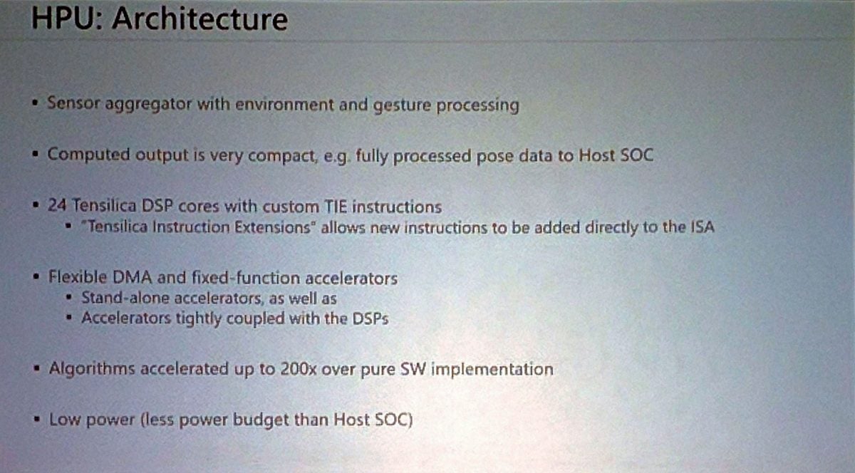
The HPU is a custom-designed TSMC-fabricated 28nm digital signal processor (DSP) with 24 Tensilica DSP cores that can process up to a trillion instructions per second with its 8 MB SRAM and 1 GB of DDR3 RAM.
The chip only takes up a 12 x 12 mm BGA package and performs 200 times faster and at lower power (only 10w) than a software-based solution.
The HPU uses the Tensilica’s instruction extensions to add 10 custom instructions to the DSPs to accelerate specific operations needed by the HoloLens and the data it delivers to the Intel Atom x86 Cherry Trail system-on-chip that powers the Windows 10 operating system is highly processed, meaning there is much less work for the Atom processor to do.
The HoloLens is currently on sale to both researchers and for commercial use for $3000. The Microsoft HoloLens Commercial Suite includes the Development Edition hardware as well as enterprise features for added security and device management. This suite acts as a solution for companies to confidently pilot and deploy HoloLens inside their organization.








User forum
14 messages